Computer Organization Theory
Introduction
High-level languages are also called algorithmic languages, oriented towards algorithms used to solve practical problems, targeting programs for processing problems and problem-solving processes.
Assembly language is the result of symbolic processing of computer machine language, with some extended functions added to facilitate programming. In assembly language, English words or abbreviations can be used to replace binary instruction codes, making them easier to remember and understand.
Machine language is a collection of instructions that computer hardware can directly recognize and execute, consisting of binary code instructions. The smallest execution unit of a program is an instruction.
Translation programs are software that translates high-level language programs into machine language programs.
- Compiler translates all statements of a high-level language program written by the user into machine language programs at once.
- Interpreter translates one statement of the source program into a corresponding machine language statement and executes it immediately.
Computer architecture refers to the computer system attributes that can be seen by programmers, i.e., conceptual structure and functional characteristics.
Computer organization refers to how to implement the attributes embodied by computer architecture, including many hardware details that are transparent to programmers.
Von Neumann Computer
- The computer consists of five major components: arithmetic unit, memory, controller, output and input devices.
- Instructions and data are stored in memory with equal status and can be accessed by address.
- Both instructions and data are represented in binary numbers.
- Instructions consist of operation codes and address codes. Operation codes represent the attributes of operations, and address codes represent the positions of operands in memory (the operand field can contain the operand itself, the operand address, or the calculation method of the operand address).
- Instructions are stored sequentially in memory and are usually executed sequentially. Under specific conditions, the execution order can be changed according to operation results or set conditions.
- The machine is centered on the arithmetic unit, and data transfer between input/output devices and memory is completed through the arithmetic unit (hence the bus).
CPU Central Processing Unit
ALU Arithmetic Logic Unit, used to complete arithmetic and logic operations.
- ACC Accumulator
- MQ Multiplier_Quotient Register
- X Operand register
CU Control Unit used to interpret instructions in memory and issue various operation commands to execute instructions.
- PC Program Counter used to store the address of the instruction to be executed currently, with a path to MAR.
- IR Instruction Register used to store the current instruction, the instruction read from MDR.
- CU Control Unit used to analyze the operations required by the current instruction and issue various micro-operation command sequences to control all controlled objects.
The execution of one instruction includes three processes: fetch, analyze, execute
- Fetch: The command register reads out an instruction
- Analyze: Analyze the instruction, indicate what operation should be completed, and specify the address of the operand according to addressing characteristics
- Execute: Complete a certain operation according to the address where the operand is located and the operation code of the instruction
MM Main Memory
- MAR Memory Address Register: used to store the address of the access unit, the number of bits represents the number of storage units.
- MDR Memory Data Register: used to store codes taken from a certain unit of the memory or codes to be stored in a certain memory.
Current CPUs integrate MAR and MDR
Machine word length refers to the number of bits that the CPU can process data at one time, usually related to the number of bits in registers.
Storage capacity = Number of storage units (MAR) × Storage word length (MDR)
Operation speed is measured by the average number of commands executed per unit time, using MIPS (Million Instructions Per Second) as the unit of measurement.
CPI Cycles Per Instruction - the number of clock cycles required to execute one instruction (reciprocal of machine frequency).
FLOPS Floating Point Operations Per Second - the number of floating point operations per second.
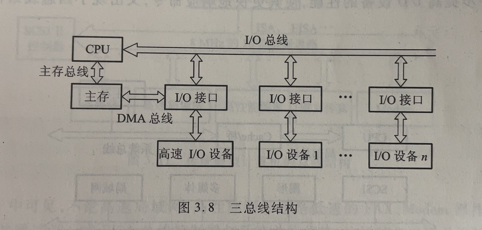
Bus
Changes between single bus and multiple buses:
- Single bus to dual bus: Separate slower I/O devices from the single bus
- Dual bus to triple bus: Connect high-speed devices in I/O bus to DMA bus
- Triple bus to quad bus: Divide main memory bus into local bus (CPU and Cache) and system bus (MM and Cache)
Bus Communication Control
Synchronous communication
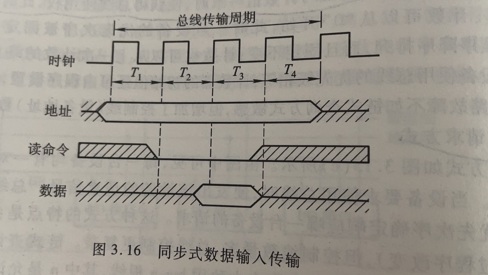 CPU sends address information on T1 rising edge; sends read command on T2 rising edge; before T3 rising edge arrives, sends the data needed by CPU to the data bus; during T3 clock cycle, sends the information on the data line to internal registers; on T4 rising edge, withdraws read command and withdraws drive to data bus.
Suitable for occasions where bus length is short and access cycles of all components are consistent
Asynchronous communication
Asynchronous communication is divided into three types: non-interlocked, semi-interlocked, and fully interlocked.
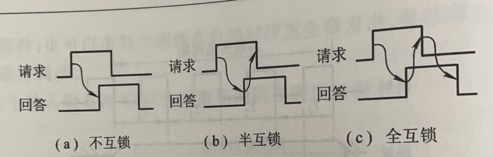 Non-interlocked: After the master module sends a request signal, it does not need to wait for the slave module's response signal, but after a period of time, after confirming that the slave module has received the request signal, it withdraws its request signal.
Semi-interlocked: The master module sends a request signal and must wait for the slave module's response signal before withdrawing its request signal, having an interlocking relationship; while the slave module sends a response signal after receiving the request signal, but does not need to wait to know that the master module's request signal has been withdrawn, but automatically withdraws the response signal after a period of time, having no interlocking relationship.
Fully interlocked: The master module sends a request signal and must wait for the slave module to respond before withdrawing its request signal; the slave module sends a response signal and must wait until it knows that the master module's request signal has been withdrawn before withdrawing its response signal.
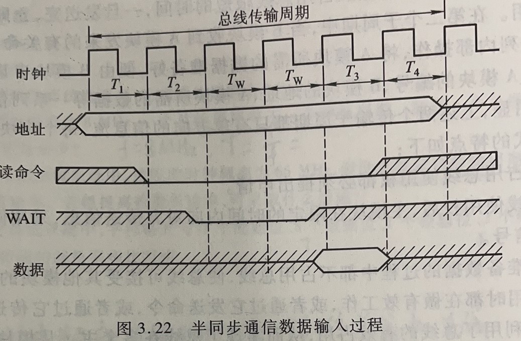 If the slave module works slowly and cannot provide data in T3 clock cycle, it must notify the master module before T3 arrives and give a low-level signal; if the master module detects a low-level signal before T3 cycle arrives, it inserts a clock cycle Tw.
Split communication omitted
Memory
RAM (Random Access Memory) - random storage, storage time is independent of the physical location of storage units.
- Static SRAM (stores information based on flip-flop principle) and Dynamic DRAM (stores information based on capacitor charge/discharge principle, needs refresh amplifier refresh every 2ms to prevent information loss)
ROM (Read Only Memory) - can only read, cannot write.
- MROM manufactured by factory, cannot be written again. At the intersection of row and column selection lines, there can be MOS transistors or none.
- PROM composed of bipolar circuits and fuses, can be written once but cannot be modified.
- EPROM uses floating gate MOS circuits, applies high voltage to drain, floating gate floats up to block circuit; erased by ultraviolet irradiation.
- EEPROM electrically erasable memory, Flash Memory
Auxiliary storage
- Magnetic disk, optical disk, magnetic tape
Cache
- cache
Serial memory - when reading and writing, it is necessary to find addresses in the order of their physical locations.
Storage capacity = Number of storage units × Storage word length (total number of bits that can store binary codes)
Storage capacity = Number of storage units × Storage word length/8 (total number of bytes that can be stored)
Storage speed
- Storage cycle (minimum interval time required for two consecutive independent storage operations, MOS 100ns TTL 10ns)
- Access time (read or write time)
Memory bandwidth - amount of information stored per unit time (T 500ns 16-bit bandwidth is 32M bits/second)
Memory and CPU Connection
Storage capacity expansion
- Bit expansion: increase storage word length
- Word expansion: increase the number of memories
- Simultaneous word and bit expansion
Address line connection: Usually connect the low bits of CPU address lines with the low bits of storage chips. The high bits of CPU are used for storage chip expansion, chip select lines, etc.
Data line connection: Must expand storage chips to make their data bits equal to CPU.
Read/write command line connection: CPU read/write command lines are generally directly connected to the read/write terminals of storage chips. Usually high level is read, low level is write.
Chip select line connection: Memory consists of many storage chips. Which chip is selected depends entirely on whether the chip select control terminal of that storage chip receives a valid chip select signal from CPU; and the chip select valid signal is related to memory access control signal (if accessing I/O, the memory access control signal is high level, indicating that memory is not required to work); high-order address lines in CPU that are not connected to storage chips must work together with memory access control signals to generate chip select signals for storage chips.
Memory Verification
For n binary bits, k verification bits are needed to form n+k bit codes satisfying: 2^k >= n + k + 1
Hamming code even parity: Only need ⊕ 1, 3, 5, 7 2, 3, 6, 7 4, 5, 6, 7 to get C1, C2, C3
Improving Memory Access Speed
Single-body multi-word system: Suitable for instructions and data stored consecutively in main memory.
Multi-body parallel system: Uses memory composed of multiple body modules. Each module has the same capacity and storage speed, and each module has independent MAR, MDR, address decoder, drive circuit and read/write circuit. They can work in parallel and interleaved.
Multi-body modules are controlled by a memory controller, which consists of a queue, control circuit, beat generator, and flag triggers.
I/O System
Program Query Method
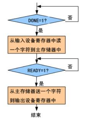
Represents the working process of inputting a character from keyboard to processor, then outputting this character to display. When DONE flag is "1", it indicates that a character has been input from keyboard to device buffer register. After this character is taken by CPU, DONE flag resets. The setting of output device flag READY is opposite to input device. When READY flag is "1", it indicates that device buffer register is empty and ready to receive data from CPU. When there is already data in device buffer register, READY flag resets, indicating that output device is outputting data from buffer register to device.
Interrupt Input/Output Method
When input device has prepared data or output device is idle, it should actively send service requests to CPU. On CPU side, after executing each instruction, it must test whether there are interrupt service requests from peripheral devices. If peripheral device interrupt service requests are found, it must temporarily stop the currently executing program, first serve peripheral devices, and continue executing original program after service completion.
The definition of interrupt input/output method is: when any exceptional events from system external, machine internal, or even processor itself occur, or although pre-arranged but appearing at unknown locations in current program, CPU suspends execution of current program, turns to handle these events, and returns to continue executing original program after processing completion.
Direct Memory Access (DMA)
For input devices:
- Read a byte or word from input medium to data buffer register BD in DMA controller. If input device is character-oriented, read characters must be assembled into words.
- If a word is not fully assembled, return to above; if verification error occurs, send interrupt request; if a word is fully assembled, send data in BD to main memory data register.
- Send address in main memory address register BA (in DMA controller) to main memory address register, and increment address in BA to next word address.
- Decrement content in data exchange count counter BC in DMA controller by "1".
- If content in BC is "0", entire DMA process ends completely, otherwise return to top to continue.
For output devices:
- Send address in main memory address register BA (in DMA controller) to main memory address register, start main memory, and increment address in BA to next word address.
- Send data in main memory data register to data buffer register BD in DMA controller. If output device is character-oriented, data in BD must be disassembled into characters.
- Write data in BD character by character (for character-oriented devices) or entire word to output medium.
- Decrement content in data exchange count counter BC in DMA controller by "1".
- If content in BC is "0", entire DMA process ends completely, otherwise return to top to continue.
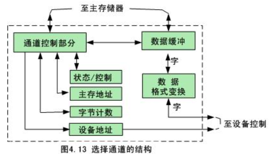
Channel Processor
-
Use supervisor instruction in user program to enter management program. CPU organizes a channel program through management program and starts channel.
-
Channel processor executes channel program organized by CPU for it, completing specified data input/output work. After channel is started, CPU can exit operating system management program, return to user program to continue executing original program, while channel begins data transfer with devices. When channel processor executes last channel instruction "disconnect channel instruction" of channel program, channel data transmission work ends completely.
-
Channel sends interrupt request to CPU after channel program ends. After CPU responds to this interrupt request, it enters operating system for second time, calling management program to handle input/output interrupt requests. If normal termination, management program performs necessary registration work. If faults, errors and other abnormal situations occur, exception handling is performed. Then CPU returns to user program to continue execution.
- Byte multiplexed channel
If various devices connected to channel take turns occupying a very short time slice (usually less than 100 microseconds) to transmit one byte, or different devices establish different transmission connections with channel logically within their allocated time slices, this is called byte-interleave mode. If a device is allowed to occupy channel for relatively long time to transmit a group of data at once, or device-channel connection can be maintained until a group of data transmission is completed as needed, this is called block mode.
- Selector channel
High-speed peripheral devices must set up dedicated channels to serve one peripheral device alone for a period of time, but can still select different devices at different times. Once a device is selected, channel enters "busy" state until data transmission work of that device is completely finished. This is selector channel.
- Array multiplexed channel
Process of reading a file from disk storage
First step is positioning, moving read/write head to track recording the file, which depends on mechanical action, called positioning time or seek time, generally requiring about ten milliseconds.
Second step is finding sector, waiting for read/write head to rotate to starting sector position recording the file, called sector finding time or waiting time. Length of waiting time mainly relates to two factors: first is disk rotation speed, second is relative distance between head position when positioned to required track and starting sector position recording the file. Therefore, waiting time length is random, maximum is time required for disk to rotate one full circle, minimum is zero. Taking average value, usually called average waiting time. Currently, high-speed disk rotation speed has reached over 5000 revolutions per minute, so average waiting time of disk storage is generally less than 10 milliseconds.
Third step is reading data. Currently, data transmission rate of high-speed disk storage has reached over 33 megabytes per second. Therefore, reading one sector (512 bytes) only takes about ten microseconds.
Array multiplexed channel logically disconnects from high-speed device immediately after issuing positioning command, reconnects when positioning is completed, issues sector finding command then disconnects again until data transmission begins. Therefore, actual working method of array multiplexed channel is: when channel is transmitting data for one high-speed device, multiple high-speed devices can be positioning or finding sectors.
Input/Output Processor
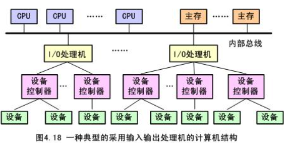 Input/output processor is usually an independent processor with certain computing functions, capable of undertaking general peripheral processor input/output, control operations and computing processing tasks. Additionally, since input/output processor has its own memory, it can complete data exchange with peripheral devices without going through main memory.
References
[^1] Computer Organization Principles Tang Shuofei Second Edition
[^2] Computer Architecture Zheng Weimin, Tang Zhizhong Second Edition
-
The code part of this work is licensed under Apache 2.0 License. Under the premise of following the license, you can freely modify and republish the code, and use the code for commercial purposes. But it requires you to:
- Attribution: In original code and derivative code, retain original author attribution and code source information.
- Retain License: In original code and derivative code, retain Apache 2.0 license file.
-
The documentation part of this work is licensed under Creative Commons Attribution 4.0 International License. Under the premise of following the license, you can freely share, including copying and distributing this work in any medium or format, and you can also freely adapt, modify, transform or create derivative works based on this work. But it requires you to:
- Attribution: When using all or part of this document, indicate the original author and source information.
- Non-commercial Use: Cannot be used for commercial publication or any other commercial activities. For commercial use, please contact the author.
- Share Alike: Works adapted and modified based on this document should continue to be licensed under Creative Commons Attribution 4.0 International License.